Board Support Package for the STM NUCLEO-H743ZI Board
Intro
DRAFT
The board support package for the STM NUCLEO-H743ZI Board is restricted to the Arduino UNO pin header and the onboard LEDs and switch (push button). The STM32H743 has much more capabilities then 16 digital I/O pins, 6 analog input pins, UART, SPI, and I2C interfaces. But if you want to use the more advanced features you can use the CubeMX to create source code for the internal peripherals. This project wants to show how to use the Cube Ecosystem for a Forth system (or vice versa) and can't implement all features and possibilities the STM32H743 has. It is a good starting point for your project.
Contents
- Overview
- Board Support Words
- Using the Digital Port Pins (Input and Output)
- Using the ADC (Analog Input Pins)
- Using the PWM (Analog Output Pins)
- Using Input Capture and Output Compare
- Using EXTI line
- Pinouts
- Digital Pins
- RESET / JP1.16
- D0 / UART_RX / PB7 / CN10.16
- D1 / UART_TX / PB6 / CN10.14
- D2 / PG14 / CN10.12
- D3 / PE13 / CN10.10
- D4 / PE14 / CN10.8
- D5 / PE11 / CN10.6
- D6 / PE9 / CN10.4
- D7 / PC13 / CN10.2
- D8 / PF3 / CN7.20
- D9 / PD15 / CN7.18
- D10 / PD14 / CN7.16
- D11 / MOSI / PB5 / CN7.14
- D12 / MISO / PA6 / CN7.12
- D13 / SCK / PA5 / CN7.10
- D14 / SDA / PB9 / CN7.4
- D15 / SCL / PB8 / CN7.2
- Analog Pins
- SD Card / SDIO Pins
- SDIO_D0 / DATA_OUT / PC8 (internal) / CN8.2
- SDIO_D1 / DAT1 / PC9 (internal) / CN8.4
- SDIO_D2 / DAT2 / PC10 (internal) / CN8.6
- SDIO_D3 / CS / PC11 (internal) / CN8.8
- SDIO_CLK / SCLK /PC12 (internal) / CN8.10
- SDIO_CMD / DATA_IN / PD2 (internal) / CN8.12
- SD_DETECT / CARD_DETECT / PB12 (internal) / optional / CN7.7
- QSPI
- USB
- VCP UART
- Digital Pins
Overview
- 256 KiB RAM dictionary
- 1024 KiB Flash dictionary
- Forth as CMSIS-RTOS thread. CMSIS-RTOS API to use FreeRTOS from Forth.
- Buffered terminal I/O (5 KiB buffer for UART Rx). Interrupt driven and RTOS aware,
keyandemitblock the calling thread.- USART1: D0 RX, D1 TX
- USART3: ST-LINK VCP
- USB-CDC for serial communication via USB. Redirect console I/O like
cdc-emit,cdc-key - microSD and internal Flash mass storage for blocks and FAT filesystem.
- Internal Flash drive 0:, e.g. W25Q128JV (16 MiB, similar to MicroSdBlocks#STM32WB_Feather)
- microSD drive 1: (optional)
- Filesystem API
- UNIX like Shell commands
- LEDs: LED1 (green, PB0), LED2 (yellow, PE1), LED3 (red, PB14)
- Switch: SW1, Push button (D7, PC13)
- Digital and analog pins, Arduino Uno Header
- Digital port pins: D0 to D15 (ST Zio D16 to D72)
- Analog port pins: A0 to A5 (ST Zio A6 to A8)
- PWM:
- TIM1: D3, D4, D5, D6
- TIM3: D11, D12
- TIM4: D0, D1, D9, D10
- Input capture TIM2: A0
- Output compare TIM2: D13
- EXTI: D11, D12, D13
- SPI: D2 SCK, D3 MISO, D4 MOSI (e.g. for display, memory)
- I2C: D14 SDA, D15 SCL (external peripherals)
- vi Editor origin in BusyBox tiny vi. Workflow development:
begin Edit EVALUATE while SaveFile repeat - Real Time Clock (32 bit UNIX time stamp, valid times are from 1.1.2000 to 31.12.2099 because of the STM32WB RTC peripheral)
time!,time@, and.time(YYYY-MM-DDTHH:MM:SS ISO 8601).
- Digital port pins D2 to D13 are inputs
- D0 (UART_RX) is input with internal pull-up resistor, D1 (UART_TX) is output
- D14 (SDA) and D15 (SCL) are open drain outputs with internal pull-up resistors
Board Support Words
led1!        ( n -- )    sets LED1 (green)
led2!        ( n -- )    sets LED2 (yellow)
led3!        ( n -- )    sets LED3 (red)
led1@        ( -- n )    gets LED1 (green)
led2@        ( -- n )    gets LED2 (yellow)
led3@        ( -- n )    gets LED3 (red)

switch1?     ( -- n )    gets switch1 (button A), closed=TRUE
dport!       ( n -- )    sets the digital output port (D0=bit0 .. D15=bit15).
dport@       ( -- n )    gets the digital input/output port (D0=bit0 .. D15=bit15).
dpin!        ( n a -- )  sets the digital output port pin a (D0=0 .. D15=15, A0=16 .. A6=23)
dpin@        ( a -- n )  gets the digital input/output port pin a
dmod         ( u a -- )  sets the pin mode: 0 in, 1 in pull-up, 2 in pull-down, 3 out push pull, 4 out open drain,
                                            5 out push pull PWM, 6 input capture, 7 output compare, 8 I2C, 9 USART, 10 analog

EXTImod      ( u a -- )  Sets for pin a (D11, D12, D13) the EXTI mode u: 0 rising, 1 falling, 2 both edges, 3 none
EXTIwait     ( u a -- )  Wait for EXTI interrupt on pin a (D11, D12, D13), timeout u in [ms]

pwmpin!      ( u a -- )  sets the digital output port pin a (D5=5, D6=6, D9=9, D10=10, D14=14, and D15=15) to a PWM value u (0..1000).
                           Default frequency is 1 kHz, TIMER3/TIMER4
pwmprescale  ( u --  )   Sets the PWM prescale for TIMER3/TIMER4. 42 kHz / prescale, default 42 -> PWM frequency 1 kHz

ICOCprescale ( u -- )    Sets the input capture / output compare prescale for TIMER2. default 42 -> 42 MHz / 42 = 1 MHz, timer resolution 1 us
ICOCperiod!  ( u -- )    Sets the input capture / output compare (TIMER2) period. default $FFFFFFFF (4'294'967'295).
                         When the up counter reaches the period, the counter is set to 0.
                         For prescale 32 the maximum time is about 1 h 11 m
ICOCcount!   ( -- u )    Sets the input capture / output compare counter for TIMER2
ICOCcount@   ( u -- )    Gets the input capture / output compare counter for TIMER2
ICOCstart    ( -- )      Starts the ICOC period
ICOCstop     ( -- )      Stops the ICOC period
OCmod        ( u a -- )  Sets for pin a (D0, D1) the Output Compare mode u: 0 frozen, 1 active level on match,
                           2 inactive level on match, 3 toggle on match, 4 forced active, 5 forced inactive

OCstart      ( u a -- )  Starts the output compare mode for pin a with pulse u
OCstop       ( a -- )    Stops output compare for pin a
ICstart      ( u -- )    Starts input capture u: 0 rising edge, 1 falling edge, 2 both edges
ICstop       ( -- )      Stops input capture

waitperiod   ( -- )      wait for the end of the TIMER2 period
OCwait       ( a -- )    wait for the end of output capture on pin a
ICwait       ( u -- u )  wait for the end of input capture with timeout u, returns counter u

apin@        ( a -- u )  gets the analog input port pin (A0=0 .. A6=6). Returns a 12 bit value (0..4095)
Using the Digital Port Pins (Input and Output)
Set 8 port pins to push/pull output3 15 dmod \ set D15 (SCL) to Output 3 5 dmod \ set D5 to Output 3 6 dmod \ set D6 to Output 3 9 dmod \ set D9 to Output 3 10 dmod \ set D10 to Output 3 11 dmod \ set D11 to output 3 12 dmod \ set D12 to output 3 13 dmod \ set D13 to outputremap D15, D5, .. D13
create port-map 15 , 5 , 6 , 9 , 10 , 11 , 12 , 13 ,

: pin ( n -- n )  \ gets the Dx pin number
  cells port-map + @
;
: left ( -- )
  7 0 do
    1 i pin dpin!
    100 osDelay drop
    0 i pin dpin!
  loop
;
|
: right ( -- )
  8 1 do
    1 8 i - pin dpin!
    100 osDelay drop
    0 8 i - pin dpin!
  loop
;
|
: knigthrider ( -- )
  begin
    left right
    key?
  until    \ key pressed
  0 0 dpin!
  key drop     \ eat key
;
|
3 16 dmod   \ set A0 to Output
3 17 dmod   \ set A1 to Output
3 18 dmod   \ set A2 to Output
3 19 dmod   \ set A3 to Output
3 20 dmod   \ set A4 to Output
3 21 dmod   \ set A5 to output
3 2 dmod    \ set D2 (SCK) to output
3 4 dmod    \ set D4 (MOSI) to output
remap D15, D5, .. D13
create port-map 16 , 17 , 18 , 19 , 20 , 21 , 2 , 4 ,
Using the ADC (Analog Input Pins)
Control the Neopixel
apin@ ( a -- u ) returns the ADC value (12 bit, 0 .. 4095) from one of the analog pins A0 to A5 (0 .. 5). Here I use the A0 to control the neopixel blue led brightness.
: neo-blue ( -- )
  begin
    0 apin@ 16 /  neopixel!
    10 osDelay drop
  key? until
  key drop
;
Control the Knightrider Pace
apin@ ( a -- u ) returns the ADC value (12 bit, 0 .. 4095) from one of the analog pins A0 to A5 (0 .. 5). Here I use the A0 to control the delay.
: left ( -- )
  7 0 do
    1 i pin dpin!
    0 apin@ 10 / osDelay drop  \ delay depends on A0
    0 i pin dpin!
  loop
;
|
: right ( -- )
  8 1 do
    1 8 i - pin dpin!
    0 apin@ 10 / osDelay drop  \ delay depends on A0
    0 8 i - pin dpin!
  loop
;
|
Using the PWM (Analog Output Pins)
Six port pins are supported so far. The 16 bit timers TIM3 (D5 and D6) and TIM4 (D9, D10, D14, and D15) are used for the timebase, time resolution is 1 us (42 MHz SysClk divided by 42). The PWM scale is from 0 (0 % duty cycle) to 1000 (100 % duty cycle), this results in a PWM frequency of 1 kHz. If you need higher PWM frequencies, decrease the divider and/or the scale. PWM port pins: D5 (TIM3CH2), D6 (TIM3CH1), D9 (TIM4CH3), D10 (TIM4CH4), D14 (TIM4CH2), and D15 (TIM4CH1). Simple test program to set brightness of a LED on pin D6 with a potentiometer on A0. Default PWM frequency is 1 kHz (prescaler set to 42). You can set the prescale with the wordpwmprescale from 42 kHz (value 1) down to 0.5 Hz (64000).
5 6 dmod   \ set D6 to PWM

: pwm ( -- )
  begin
    0 apin@  4 /  6 pwmpin!
    10 osDelay drop
    key?
  until
  key drop
;
Control an RC Servo
https://en.wikipedia.org/wiki/Servo_(radio_control| 0° | 1 ms | 50 |
| 45° | 1.5 ms | 75 |
| 90° | 2 ms | 100 |
| 180° | 3 ms | 150 |
| 270 | 4 ms | 200 |
| 0° | 1 ms | 50 |
| 90° | 1.5 ms | 75 |
| 180° | 2 ms | 100 |
| 270° | 2.5 ms | 150 |
840 pwmprescale
5 5 dmod   \ set D5 to PWM

: servo ( -- )
  begin
    130 40 do
      i 5 pwmpin!
      i neopixel!
      i 40 = if
        1000 \ give some more time to get back
      else
        200
      then
      osDelay drop
    10 +loop
  key? until
  key drop
;
Using Input Capture and Output Compare
Time Base
Default timer resolution is 1 us. The 32 bit TIMER2 is used as time base for Input Capture / Output Compare. For a 5 s period 5'000'000 cycles are needed. All channels (input capture / output compare) use the same time base.
: period ( -- )
  5000000 ICOCperiod! \ 5 s period
  ICOCstart
  begin
     waitperiod
     cr .time
  key? until
  key drop
;
Output Compare
Output compare TIM2: D0, D1
7 0 dmod  \ output compare for D0
7 1 dmod  \ output compare for D1

: oc-toggle ( -- )
  5000000 ICOCperiod! \ 5 s period
  ICOCstart
  3 0 OCmod  1000000 0 OCstart \ toggle D0 after 1 s
  3 1 OCmod  2000000 1 OCstart \ toggle D1 after 2 s
  begin
     waitperiod
     cr .time
  key? until
  key drop
;
When you abort (hit any key) the program, the timer still runs and controls the port pins. To stop the port pins:
0 OCstop 1 OCstopOr change the prescale to make it faster or slower:
1 ICOCprescale
Input Capture
This sample program measures the time between the edges on port A1. if no event occurs within 2 seconds, "timeout" is issued. Hit any key to abort program.
: ic-test ( -- )
  6 17 dmod \ input capture on A1
  ICOCstart
  2 ICstart  \ both edges
  ICOCcount@ ( -- count )
  begin
    2000 \ 2 s timeout
    ICwait ( -- old-capture capture )
    cr
    dup 0= if
      ." timeout" drop
    else
      dup rot ( -- capture capture old-capture )
      - 1000 / . ." ms"
    then
  key? until
  key drop
  drop
  ICstop
;
Using EXTI line
D11, D12, and D13 can be used as an EXTI line. EXTIs are external interrupt lines, D13 uses EXTI1 (EXTI Line1 interrupt), D12 EXIT2, and D11 EXTI3.
: exti-test ( -- )
  2 11 EXTImod \ both edges on D11
  begin
    2000 11 EXTIwait \ wait for edge on D11 with 2 s timeout
    cr
    0= if
      11 dpin@ if
        ." rising edge"
      else
        ." falling edge"
      then
    else
      ." timeout"
    then
  key? until
  key drop
;
Pinouts
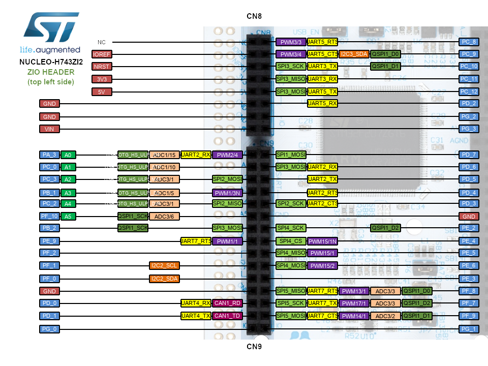
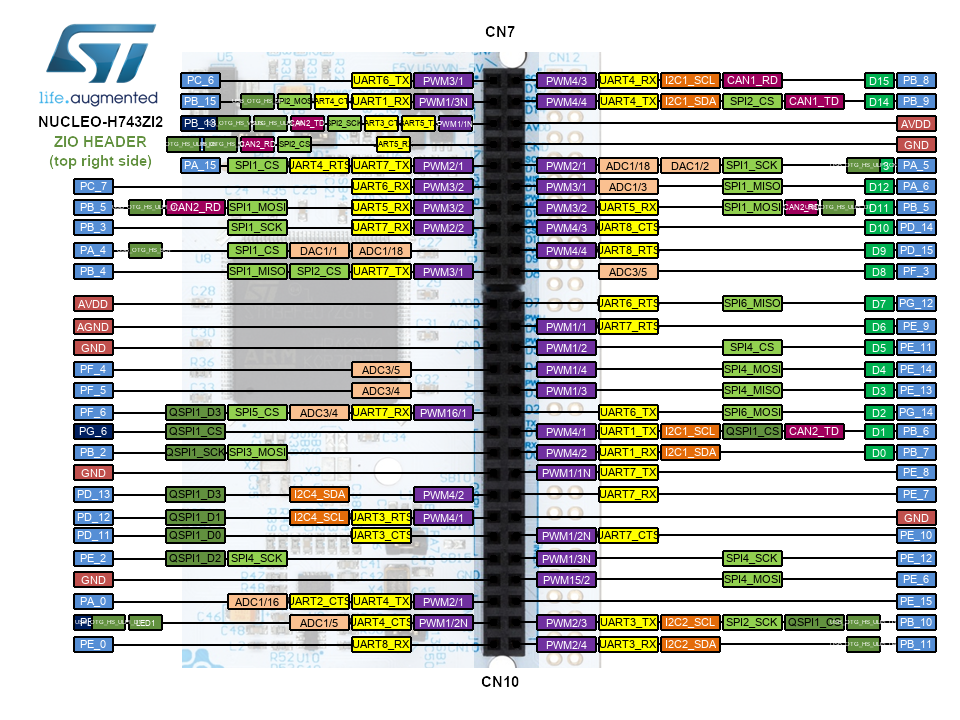
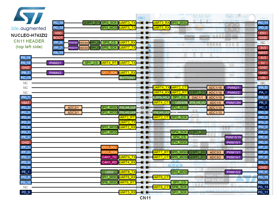
SCL D15, SDA D14
SCK D2, MO D4, MI D3, RX D0, TX D1
The anlog pins can be used as digital pins too:
A0 D16, A1 D17, A2 D18, A3 D19, A4 D20, A5 D21
Digital Pins
RESET / JP1.16
D0 / UART_RX / PB7 / CN10.16
- Receive (input) pin for Serial1. Hardware USART1_RX
- PWM out on TIM4_CH2
- Alternate uses: I2C1_SDA
D1 / UART_TX / PB6 / CN10.14
- Transmit (output) pin for Serial1. Hardware USART1_TX
- PWM out on TIM4_CH1
- Alternate uses: I2C1_SCL
D2 / PG14 / CN10.12
- Alternate uses: UART6_TX, SPI6_MOSI
D3 / PE13 / CN10.10
- PWM out on TIM1_CH3
- Alternate uses: SPI6_MISO
D4 / PE14 / CN10.8
- PWM out on TIM1_CH4
- Alternate uses: SPI4_MOSI
D5 / PE11 / CN10.6
- PWM out on TIM1_CH2
- Alternate uses: USART6_RX
D6 / PE9 / CN10.4
- PWM out on TIM1_CH1
- Alternate uses: USART6_TX
D7 / PC13 / CN10.2
- Blue Button
- Alternate uses: SPI6_MISO, USART6_RTS
D8 / PF3 / CN7.20
- Alternate uses: ADC3_5
D9 / PD15 / CN7.18
- PWM out on TIM4_CH4
- Alternate uses: UART8_RTS
D10 / PD14 / CN7.16
- PWM out on TIM4_CH3
- Alternate uses: UART8_CTS, SPI1_CS
D11 / MOSI / PB5 / CN7.14
- SPI SPI1_MOSI
- PWM out on TIM3_CH2
- Alternate uses: USART5_RX
D12 / MISO / PA6 / CN7.12
- SPI SPI1_MISO
- PWM out on TIM3_CH1
- Alternate uses: I2S2ext SD, SPI2 MISO
D13 / SCK / PA5 / CN7.10
- SPI SPI1_SCK
- Output Compare on TIM2_CH1
- Alternate uses: ADC1_8
D14 / SDA / PB9 / CN7.4
D15 / SCL / PB8 / CN7.2
Analog Pins
A0 / D16 / PA3 / CN9.1
- This pin is analog input A0 (ADC1_IN15)
- Input Capture on TIM2_CH4
- Alternate uses: USART2_RX
A1 / D17 / PC0 / CN9.3
- This pin is analog input A1 (ADC1_IN10)
A2 / D18 / PC3 / CN9.5
- This pin is analog input A2 (ADC3_IN1)
- PWM out on TIM1_CH3N
A3 / D19 / PB1 / CN9.7
- This pin is analog input A3 (ADC1_IN5)
- PWM out on TIM3_CH2
A4 / D20 / PC2 / CN9.9
- This pin is analog input A4 (ADC3_IN0)
A5 / D21 / PF10 / CN9.11
- This pin is analog input A5 (ADC3_IN6)
SD Card / SDIO Pins
SDIO_D0 / DATA_OUT / PC8 (internal) / CN8.2
SDIO_D1 / DAT1 / PC9 (internal) / CN8.4
SDIO_D2 / DAT2 / PC10 (internal) / CN8.6
SDIO_D3 / CS / PC11 (internal) / CN8.8
SDIO_CLK / SCLK /PC12 (internal) / CN8.10
SDIO_CMD / DATA_IN / PD2 (internal) / CN8.12
SD_DETECT / CARD_DETECT / PB12 (internal) / optional / CN7.7
QSPI
QS_CS / PG6 (external) / CN10.13
QS_CLK / PB2 (external) / CN10.15
QS_D3 / PD13 (external) / CN10.19
QS_D1 / PD12 (external) / CN10.21
QS_D0 / PD11 (external) / CN10.23
QS_D2 / PE2 (external) / CN10.25
USB
USB_DP / PA12
USB_DM / PA11
VCP UART
STLK_VCP_TX / PG14 / ST-LINK VCP Rx
- USART3_TX
STLK_VCP_RX / PG9 / ST-LINK VCP Tx
- USART3_RX

This work by Peter Schmid is licensed under a Creative Commons Attribution-ShareAlike 4.0 International License.
Topic revision: r9 - 2022-06-27 - PeterSchmid

|
|
|
|
Ideas, requests, problems regarding TWiki? Send feedback