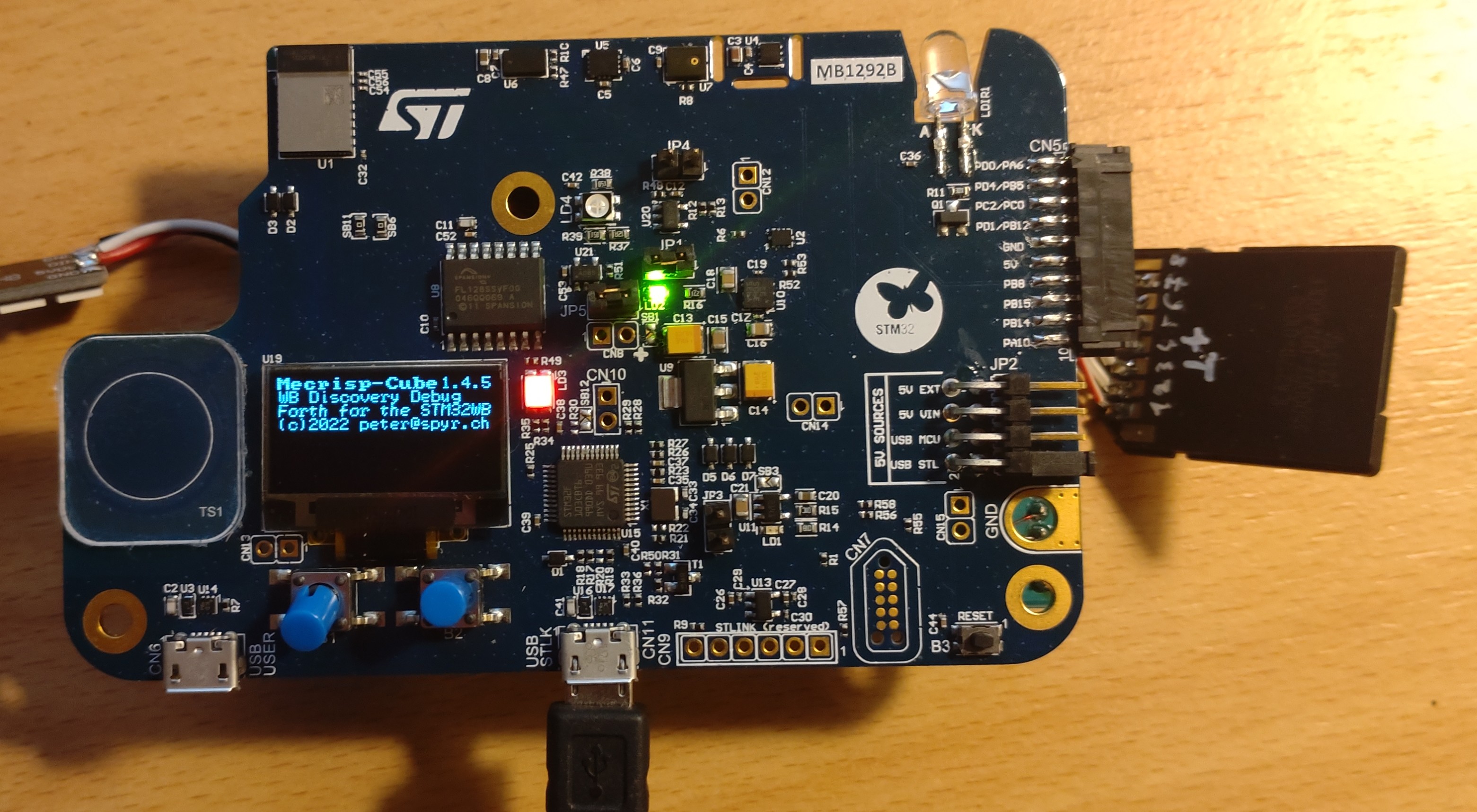
Board Support Package for the STM32WB5MM-DK Discovery Kit
Intro
The board support package for the STM32WB5MM-DK Discovery Kit is restricted to the Arduino UNO R3 pin header and the onboard LEDs, and switches (buttons). The STM32 has much more capabilities then 14 digital I/O pins, 6 analog input pins, UART, SPI, and I2C interfaces. But if you want to use the more advanced features you can use the CubeMX to create source code for the internal peripherals. This project wants to show how to use the Cube Ecosystem for a Forth system (or vice versa) and can't implement all features and possibilities the STM32WB has. It is a good starting point for your project.

 This page is no longer updated regularly, the current documentation can be found at
GitHub
This page is no longer updated regularly, the current documentation can be found at
GitHub .
.
Board Support Words
Defaults: Digital port pins D0 to D7 are push pull outputs, D8 to D15 are inputs with pull-up resistors.
rgbled!      ( rgb -- )  sets the RGB led ($ff0000 red, $00ff00 green, $0000ff blue)

switch1?     ( -- n )    gets switch1, closed=TRUE
switch2?     ( -- n )    gets switch2, closed=TRUE

dport!       ( n -- )    sets the digital output port (D0=bit0 .. D15=bit15).
dport@       ( -- n )    gets the digital input/output port (D0=bit0 .. D15=bit15).
dpin!        ( n a -- )  sets the digital output port pin (a: D0=0 .. D15=15, A0=16 .. A5=21)
dpin@        ( a -- n )  gets the digital input/output port pin (a: D0=0 .. D15=15, A0=16 .. A5=21)
dmod         ( u a -- )  sets the pin mode: 0 in, 1 in pull-up, 2 in pull-down, 3 out push pull, 4 out open drain,
                                            5 out push pull PWM, 6 input capture, 7 output compare, 8 I2C, 9 UART, 10 analog

EXTImod      ( u a -- )  Sets for pin a (D0, D1, D2, D4, D10) the EXTI mode u: 0 rising, 1 falling, 2 both edges, 3 none
EXTIwait     ( u a -- )  Wait for EXTI interrupt on pin a (D0, D1, D2, D4, D10), timeout u in [ms]

pwmpin!      ( u a -- )  sets the digital output port pin a (D3=3, D6=6, D9=9) to a PWM value u (0..1000). Default frequency is 1 kHz, TIMER1
pwmprescale  ( u --  )   Sets the PWM prescale for TIMER1 and TIMER16. 32 kHz / prescale, default 32 -> PWM frequency 1 kHz

ICOCprescale ( u -- )    Sets the input capture / output compare prescale for TIMER2. default 32 -> 32 MHz / 32 = 1 MHz, timer resolution 1 us
ICOCperiod!  ( u -- )    Sets the input capture / output compare (TIMER2) period. default $FFFFFFFF (4'294'967'295).
                         When the up counter reaches the period, the counter is set to 0.
                         For prescale 32 the maximum time is about 1 h 11 m
ICOCcount!   ( -- u )    Sets the input capture / output compare counter for TIMER2
ICOCcount@   ( u -- )    Gets the input capture / output compare counter for TIMER2
ICOCstart    ( -- )      Starts the ICOC period
ICOCstop     ( -- )      Stops the ICOC period
OCmod        ( u a -- )  Sets for pin a (D5, D13) the Output Compare mode u: 0 frozen, 1 active level on match, 2 inactive level on match,
                            3 toggle on match, 4 forced active, 5 forced inactive

OCstart      ( u a -- )  Starts the output compare mode for pin a with pulse u
OCstop       ( a -- )    Stops output compare for pin a
ICstart      ( u -- )    Starts input capture u: 0 rising edge, 1 falling edge, 2 both edges
ICstop       ( -- )      Stops input capture

waitperiod   ( -- )      wait for the end of the TIMER2 period
OCwait       ( a -- )    wait for the end of output capture on pin a
ICwait       ( u -- u )  wait for the end of input capture with timeout u, returns counter u

apin@        ( a -- u )  gets the analog input port pin (A0 .. A5). Returns a 12 bit value (0..4095)

I2Cdev       ( u -- )           Sets the 7-bit I2C address
I2Cput       ( c-addr u -- )    put a message with length u from buffer at c-addr to the I2C slave device
I2Cget       ( c-addr u -- )    get a message with length u from I2C slave device to buffer at c-addr
I2Cputget    ( a1 u1 a2 u2 -- ) put a message with length u1 from buffer at a1 to the I2C slave device
                                and get a message with length u2 from device to buffer at a2

SPIputget    ( a1 a2 u -- )     put a message with length u from buffer at a1 to the SPI slave device
                                and get a message with length u from device to buffer at a2
SPIputc      ( char )           put a single char to the SPI slave device
Using the Digital Port Pins (Input and Output)
This example is very similar to the McForth#Knight_Rider program.dport! and dport@ set and get all 16 digital pins (D0 to D15) at once. You have to press the SW1 push button til D0 is set to cancel the operation.
3 0 dmod   \ set D0 to Output
3 1 dmod   \ set D1 to Output
3 2 dmod   \ set D2 to Output
3 3 dmod   \ set D3 to Output
3 4 dmod   \ set D4 to Output
3 5 dmod   \ set D5 to Output
3 6 dmod   \ set D6 to Output
3 7 dmod   \ set D7 to Output
: left ( -- )
  7 0 do
    dport@ shl dport!
    100 osDelay drop
  loop
;
|
: right ( -- )
  7 0 do
    dport@ shr dport!
    100 osDelay drop
  loop
;
|
: knightrider ( -- )
  1 dport!
  begin
    left right
    switch1? \ or key?
  until
  0 dport!
;
|
: left ( -- )
  7 0 do
    1 i dpin!
    100 osDelay drop
    0 i dpin!
  loop
;
|
: right ( -- )
  8 1 do
    1 8 i - dpin!
    100 osDelay drop
    0 8 i - dpin!
  loop
;
|
: knigthrider ( -- )
  begin
    left right
    switch1?
  until
  0 0 dpin!
;
|
Using the ADC (Analog Input Pins)
apin@ ( a -- u ) returns the ADC value (12 bit, 0 .. 4095) from one of the analog pins A0 to A5 (0 .. 5). Here I use the A0 to control the delay.
: left ( -- )
  7 0 do
    1 i dpin!
    0 apin@ 10 / osDelay drop  \ delay depends on A0
    0 i dpin!
  loop
;
|
: right ( -- )
  8 1 do
    1 8 i - dpin!
    0 apin@ 10 / osDelay drop  \ delay depends on A0
    0 8 i - dpin!
  loop
;
|
left or right word takes about 125 us, the knightrider loop about 50 us (no osDelay). Pretty fast for my opinion.
CH1 yellow: D0 pinCH2 blue: D1 pin

Using the PWM (Analog Output Pins)
Only three port pins are supported so far. The 16 bit TIMER1 is used for the timebase, time resolution is 1 us (32 MHz SysClk divided by 32). The PWM scale is from 0 (0 % duty cycle) to 1000 (100 % duty cycle), this results in a PWM frequency of 1 kHz. If you need higher PWM frequencies, decrease the divider and/or the scale. PWM port pins: D6 (TIM1CH1), D9 (TIM1CH2), D3 (TIM1CH3) Simple test program to set brightness of a LED on pin D3 with a potentiometer on A0. Default PWM frequency is 1 kHz (prescaler set to 32). You can set the prescale with the wordpwmprescale from 32 kHz (value 1) down to 0.5 Hz (64000).
5 3 dmod   \ set D3 to PWM

: pwm ( -- )
  begin
    0 apin@  4 /  3 pwmpin!
    10 osDelay drop
    switch1?
  until
;
Using Input Capture and Output Compare
Time Base
Default timer resolution is 1 us. The 32 bit TIMER2 is used as time base for Input Capture / Output Compare. For a 5 s period 5'000'000 cycles are needed. All channels (input capture / output compare) use the same time base.
: period ( -- )
  5000000 ICOCperiod! \ 5 s period
  ICOCstart
  begin
     waitperiod
     cr .time
  key? until
  key drop
;
Output Compare
: oc-toggle ( -- )
  5000000 ICOCperiod! \ 5 s period
  ICOCstart
  3 0 OCmod  1000000 0 OCstart \ toggle D0 after 1 s
  3 1 OCmod  2000000 1 OCstart \ toggle D1 after 2 s
  3 5 OCmod  3000000 5 OCstart \ toggle D5 after 3 s
  begin
     waitperiod
     cr .time
  key? until
  key drop
;
When you abort (hit any key) the program, the timer still runs and controls the port pins. To stop the port pins:
0 OCstop 1 OCstop 5 OCstopOr change the prescale to make it faster or slower:
1 ICOCprescale
Input Capture
This sample program measures the time between the edges on port A2. if no event occurs within 2 seconds, "timeout" is issued. Hit any key to abort program.
: ic-test ( -- )
  6 2 dmod \ input capture on A2
  ICOCstart
  2 ICstart  \ both edges
  ICOCcount@ ( -- count )
  begin
    2000 \ 2 s timeout
    ICwait ( -- old-capture capture )
    cr
    dup 0= if
      ." timeout" drop
    else
      dup rot ( -- capture capture old-capture )
      - 1000 / . ." ms"
    then
  key? until
  key drop
  drop
  ICstop
;
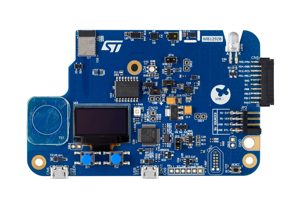
Pinouts
SchematicsARDUINO® Connector Pinout
| Connector | Signal name | STM32W5MMG pin | Comment |
|---|---|---|---|
| CN2.1 | NC | - | NC (reserved for the test) |
| CN2.2 | 3V3 (IOREF) | - | IOREF 3V3 |
| CN2.3 | NRST | NRST | NRST |
| CN2.4 | 3V3 | - | 3.3 V |
| CN2.5 | 5V | - | 5 V |
| CN2.6 | GND | - | Ground |
| CN2.7 | GND | - | Ground |
| CN2.8 | VIN | Ext. +12V | |
| CN3.1 | A0 | PC3 | ADC1_IN4 |
| CN3.2 | A1 | PA2 | ADC1_IN7/TIM2_CH1 IC |
| CN3.3 | A2 | PA5 | ADC1_IN10 |
| CN3.4 | A3 | PC1 | ADC1_IN2 |
| CN3.5 | A4 | PC4 | ADC1_IN13 |
| CN3.6 | A5 | PC5 | ADC1_IN14 |
| CN4.1 | D0 | PC0 | LPUART1_RX/EXTI0 |
| CN4.2 | D1 | PB5 | LPUART1_TX/EXTI9_5 |
| CN4.3 | D2 | PD12 | GPIO/EXTI15_10 |
| CN4.4 | D3 | PD14 | GPIO/TIM1_CH1 |
| CN4.5 | D4 | PE3 | GPIO/EXTI_3 |
| CN4.6 | D5 | PB10 | GPIO/TIM2_CH3 OC |
| CN4.7 | D6 | PE0 | GPIO/TIM16_CH1 |
| CN4.8 | D7 | PB2 | GPIO |
| CN1.1 | D8 | PD13 | GPIO |
| CN1.2 | D9 | PD15 | GPIO/TIM1_CH2 |
| CN1.3 | D10 | PA4 | SPI1_NSS/EXTI4 |
| CN1.4 | D11 | PA7 | SPI1_MOSI |
| CN1.5 | D12 | PB4 | SPI1_MISO |
| CN1.6 | D13 | PA1 | SPI1_SCK/TIM2_CH2 OC |
| CN1.7 | GND | - | Ground |
| CN1.8 | AVDD | - | VDDA |
| CN1.9 | D14 | PA10 | I2C1_SDA |
| CN1.10 | D15 | PB8 | I2C1_SCL |
| GPIO_SELECT1 | PE2 | 0 IR LED, 1 RGB LED | |
| GPIO_SELECT2 | PH1 | 0 STMOD+, 1 LPUART D0/D1 |
Push Buttons
| Signal name | STM32W5MMG pin | Comment |
|---|---|---|
| SWITCH1 | PC12 | WKUP3 |
| SWITCH2 | PC13 | WKUP2 |
RGB LED
| Signal name | STM32W5MMG pin | Comment |
|---|---|---|
| D11 | PA7 | SPI1_MOSI |
| RGB_SELECT | PH1 | RGB CS |
UART VCP ST-LINK
| Signal name | STM32W5MMG pin | Comment |
|---|---|---|
| UART_TX | PB6 | USART1_TX |
| UART_RX | PB7 | USART1_RX |
Quad SPI for Flash
| Signal name | STM32W5MMG pin | Comment |
|---|---|---|
| FLASH_NCS | PD3 | QUADSPI_BK1_NCS |
| FLASH_IO0 | PB9 | QUADSPI_BK1_IO0 |
| FLASH_IO1 | PD5 | QUADSPI_BK1_IO1 |
| FLASH_IO2 | PD6 | QUADSPI_BK1_IO2 |
| FLASH_IO3 | PD7 | QUADSPI_BK1_IO3 |
| FLASH_SCLK | PA3 | QUADSPI_BK1_SCLK |
- 256- or 512-byte page programming buffer options
- Quad-input page programming (QPP) for slow clock systems
- Automatic ECC-internal hardware error correction code generation with single bit error correction
- Hybrid sector size option - Physical set of thirty two 4-KB sectors at top or bottom of address space with all remaining sectors of 64 KB :-(, for compatibility with prior generation S25FL devices.
- Uniform sector option - always erase 256-KB blocks for software compatibility with higher density and future devices.
SPI OLED Display
| Signal name | STM32W5MMG pin | Comment |
|---|---|---|
| D13 | PA1 | SPI1_SCK |
| D12 | PB4 | SPI1_MISO |
| D11 | PA7 | SPI1_MOSI |
| OLED_CS | PH0 | SPI1_NSS |
| OLED_RST | PC8 | Reset OLED |
| OLED_DC | PC9 | Data/Control |
- https://github.com/STMicroelectronics/stm32-ssd1315/blob/main/ssd1315.c
- https://files.seeedstudio.com/wiki/Grove-OLED-Display-0.96-SSD1315-/res/OEL%20Display%20Module.pdf
Onboard Mems (I2C)
| Signal name | STM32W5MMG pin | Comment |
|---|---|---|
| MEMS_SCK | PB13 | I2C3_SCL |
| MEMS_SDA | PB11 | I2C3_SDA |
| MEMS_INT | PD2 | Accelerometer, Gyro |
| MEMS_RDY | PE1 | STTS22H temperatrur sensor |
Digital Microphone
| Signal name | STM32W5MMG pin | Comment |
|---|---|---|
| MICRO_CK | PA8 | SAI1_CK2 |
| MICRO_DI | PA9 | SAI1_DI2 |
STMod+ Connector Pinout
| Connector | Signal name | STM32W5MMG pin | Comment |
|---|---|---|---|
| CN5.1 | PD0, PA6 | SPI2_NSS, LPUART1_CTS | |
| CN5.2 | , D1 | PD4, PB5 | SPI2_MOSI (1), LPUART1_TXD |
| CN5.3 | , D0 | PC2, PC0 | SPI2_MISO (1), LPUART1_RXD |
| CN5.4 | PD1, PB12 | SPI2_SCK, LPUART1_RTS | |
| CN5.5 | GND | Ground | |
| CN5.6 | +5V | Power | |
| CN5.7 | D15 | PB8 | I2C1_SCL |
| CN5.8 | PB15 | SPI2_MOSI (2) | |
| CN5.9 | PB14 | SPI2_MISO (2) | |
| CN5.10 | D14 | PA10 | I2C1_SDA |
| CN5.11 | PE3 | INT | |
| CN5.12 | PD8 | STMOD+_RESET | |
| CN5.13 | PA0 | ADC1_IN5 | |
| CN5.14 | PA15 | PWM (TIM2_CH1) | |
| CN5.15 | +5V | Power | |
| CN5.16 | GND | Ground | |
| CN5.17 | PC11 | GPIO | |
| CN5.18 | PC10 | GPIO | |
| CN5.19 | PA5 | GPIO, ADC1_IN10 | |
| CN5.20 | A3 | PC1 | GPIO, ADC1_IN12 |

This work by Peter Schmid is licensed under a Creative Commons Attribution-ShareAlike 4.0 International License.


| I | Attachment | History | Action | Size | Date | Who | Comment |
|---|---|---|---|---|---|---|---|
| |
stm32wb-discovery.jpg | r1 | manage | 408.9 K | 2021-06-25 - 10:00 | PeterSchmid | |
| |
wb55-discovery-clip.jpg | r1 | manage | 883.1 K | 2022-09-29 - 18:52 | PeterSchmid | |
| |
wb55-discovery-header.jpg | r1 | manage | 49.3 K | 2022-09-29 - 18:59 | PeterSchmid |
Topic revision: r16 - 2024-02-17 - PeterSchmid

Ideas, requests, problems regarding TWiki? Send feedback